
This document provides information about QFET components.
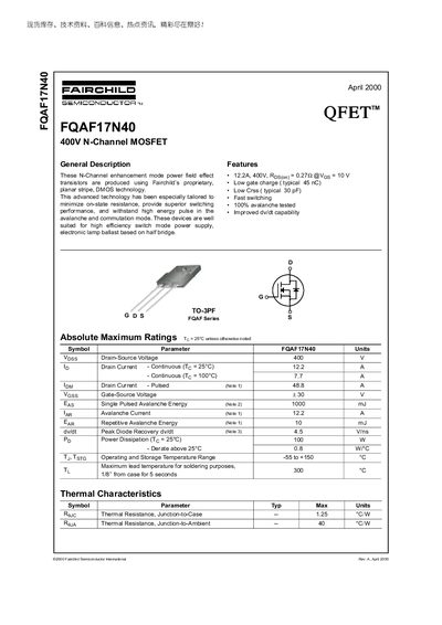
The FQAF17N40 is a 400 V N‑Channel enhancement mode power MOSFET designed with Fairchild's planar stripe DMOS technology for low on‑state resistance, low gate charge, and fast switching. It is intended for high‑efficiency switch‑mode power supplies and lamp ballast applications.
Key specifications include a continuous drain current of 12.2 A at 25 °C, pulsed current capability of 48.8 A, gate‑source voltage rating of ±30 V, and a power dissipation rating of 100 W. The device is supplied in a TO‑3PF package with detailed thermal resistance values and includes test circuit diagrams for gate charge and diode recovery characteristics.
| Drain-Source Voltage (V_DSS) | 400 V |
|---|---|
| Continuous Drain Current (I_D) @25°C | 12.2 A |
| Pulsed Drain Current (I_D(pulsed)) | 48.8 A |
| Gate-Source Voltage (V_GS) | ±30 V |
| Power Dissipation (P_D) @25°C | 100 W |
| Junction-to-Case Thermal Resistance (RθJC) | 1.25 °C·W |
| Junction-to-Ambient Thermal Resistance (RθJA) | 40 °C·W |
| Typical Gate Charge | 45 nC |
The device is rated for a maximum drain‑source voltage of 400 V.
The typical gate charge is about 45 nC.
No, Fairchild does not authorize its use in life‑support systems without written approval.