
This document introduces the TC7WG00FU/FK product from Dinghao Corporation, which is a CMOS digital integrated circuit with dual 2-input NAND gate. The product features high-speed operation, high-level output current, wide operating voltage range, etc.
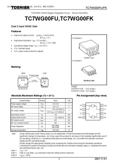
The Toshiba TC7WGOOFU/FK is a dual 2‑input NAND gate CMOS integrated circuit. It offers high‑level output current of up to 8 mA at 3 V, a typical propagation delay of 2.5 ns at 3.3 V with 15 pF load, and operates over a supply range of 0.9 V to 3.6 V. The device is supplied in SSOP‑8 packages (0.65 mm and 0.50 mm pitch) with typical weights of 0.02 g and 0.01 g respectively.
The document provides detailed electrical characteristics, pin assignments, package dimensions, and usage restrictions. It notes that the IC is intended for general electronics applications and should not be used in safety‑critical or high‑reliability systems such as medical, aerospace, or traffic control equipment.