
TC7WG04FU/FK is a triple inverter produced by Toshiba Corporation. Its operating voltage range is 0.9~3.6V, output current is ±8mA, input voltage range is -0.5~7V, and maximum input voltage is 5.5V and maximum output voltage is 3.6V.
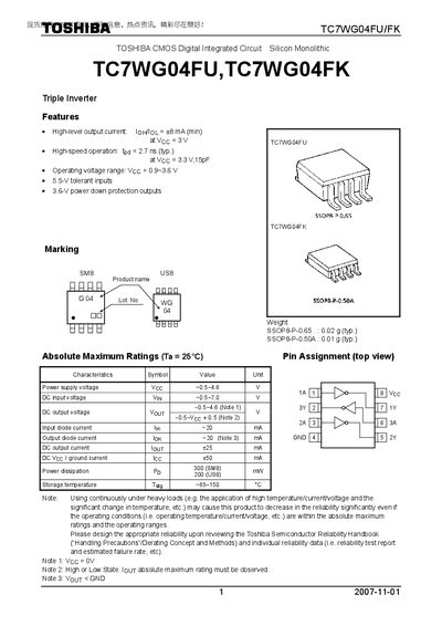
The TC7WG04FU and TC7WG04FK are Toshiba CMOS digital integrated circuits that implement a triple inverter. The device offers high‑level output current, high‑speed operation (tpd ≈ 2.7 ns) and operates from 0.9 V to 3.6 V supply voltage. Key features include 5.5‑V tolerant inputs and power‑down protection on the outputs.
The document provides absolute maximum ratings, detailed DC and AC electrical characteristics, pin‑out information, and mechanical data for the SSOP‑8 packages (0.65 mm and 0.50 mm pitch). It also contains a disclaimer on product use, specifying that the parts are not intended for safety‑critical or high‑reliability applications such as aerospace, medical or traffic‑control equipment.
| Operating voltage range | 0.9 V – 3.6 V |
|---|---|
| High‑level output current (minimum) | 8 mA |
| DC output current (typical max) | 25 mA |
| Package weight (SSOP8‑P‑0.65) | 0.02 g (typ.) |
The device operates from 0.9 V up to 3.6 V supply voltage.
The datasheet specifies a typical maximum DC output current of 25 mA.
Yes, the part is not intended for use in safety‑critical or high‑reliability applications such as aerospace, medical or traffic‑signal equipment.
The SSOP8‑P‑0.65 package weighs 0.02 g (typical).