
This document is a datasheet for Toshiba TC7WG125FC, which introduces the features of the product, including high-level output current, high-speed operation, operating voltage range, 5.5V tolerant inputs and 3.6V power down protection outputs.
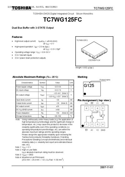
The TC7WG125FC is a CMOS dual‑bus buffer with 3‑state output designed for high‑speed operation in general electronics applications. It offers high‑level output current of up to +8 mA and operates over a wide voltage range.
Key specifications include a typical propagation delay of 2.5 ns, a power dissipation of 150 mW, and a compact CSON8‑P‑0.4 package weighing 0.002 g. The document also outlines recommended usage restrictions and reliability guidelines for safe system design.
| High‑level output current | +8 mA (min) at Vcc = 3 V |
|---|---|
| Propagation delay (tpd) | 2.5 ns (typ.) at Vcc = 3.3 V, 15 pF |
| Operating voltage range | 0.9 V ~ 3.6 V |
| Power dissipation | 150 mW |
| Storage temperature | -65 °C ~ 150 °C |
| Package weight | 0.002 g (typ.) |
The device operates from 0.9 V to 3.6 V supply voltage.
It can source up to +8 mA (minimum) at a 3 V supply.
Yes, it is not intended for safety‑critical or high‑reliability applications such as medical, aerospace, or traffic control equipment.