
This document describes the features of the TC7WG02FC model, including high-level output current, high-speed operation, operating voltage range, input and output voltage, etc.
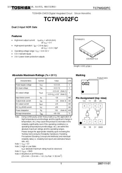
The TC7WG02FC is a Toshiba CMOS dual 2‑input NOR gate designed for general electronics applications. It offers high‑level output current of up to +8 mA, a typical propagation delay of 2.8 ns, and operates over a wide supply range of 0.9 V to 3.6 V.
The document provides detailed electrical specifications, package dimensions, and important usage restrictions, noting that the device is not intended for safety‑critical or high‑reliability systems such as medical or aerospace equipment.
| Propagation delay (tpd) | 2.8 ns (typ.) at Vcc = 3.3 V, 15 pF |
|---|---|
| Operating voltage range | 0.9 V ~ 3.6 V |
The typical propagation delay is 2.8 ns measured at a supply voltage of 3.3 V with a 15 pF load.
The device operates correctly with a supply voltage between 0.9 V and 3.6 V.
Yes, the device is not intended for use in equipment where failure could cause loss of life or serious injury, such as medical, aerospace, or safety‑critical systems.