
TC7WG125FC is a TOSHIBA CMOS digital integrated circuit with dual bus buffer and 3-STATE output features. It has high-level output current, high-speed operation, operating voltage range, 5.5V tolerant inputs, and 3.6V power down protection outputs.
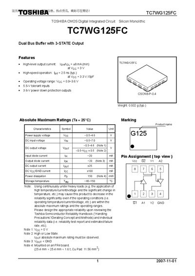
The TC7WG125FC is a CMOS dual‑bus buffer with 3‑state output, designed for high‑speed operation and low‑power consumption. It features a high‑level output current of up to +8 mA and operates over a wide voltage range.
The document lists detailed DC and AC electrical characteristics, package dimensions, and important handling and reliability notes. It also defines prohibited applications such as medical, aerospace, and safety‑critical equipment.
| Operating voltage range | 0.9 V ~ 3.6 V |
|---|---|
| High‑level output current | +8 mA (min) |
| Propagation delay (typ.) | 2.5 ns |
| Package dimensions | 1.35 mm × 0.05 mm |
| Weight (typ.) | 0.002 g |
The device operates from 0.9 V to 3.6 V supply voltage.
Typical propagation delay is 2.5 ns.
The high‑level output current is specified as +8 mA minimum.