
The ADN2807 is a 155/622 Mb/s clock and data recovery IC with integrated limiting amp for SONET OC-3/-12, SDH STM-1/-4 and 15/14 FEC networks.
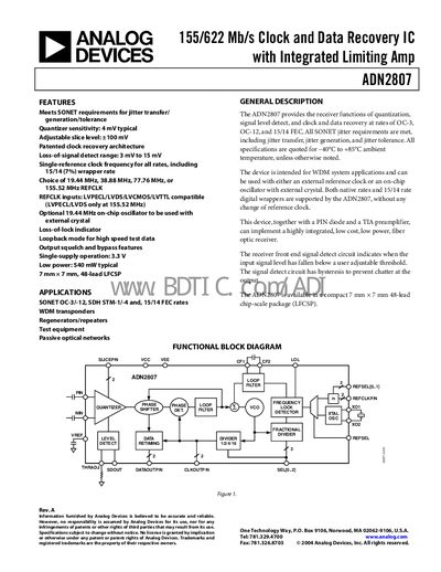
The ADN2807 provides receiver functions for quantization, signal‑level detection, and clock‑and‑data recovery at OC‑3, OC‑12 and 15/14 FEC rates. It meets all SONET jitter requirements, supports single‑supply 3.3 V operation, and offers selectable reference clock frequencies of 19.44 MHz, 38.88 MHz, 77.76 MHz or 155.52 MHz.
The device is supplied in a compact 7 mm × 7 mm 48‑lead LFCSP package and is intended for WDM system applications such as transponders, regenerators, test equipment and passive optical networks. Detailed specifications cover input voltage ranges, power consumption, jitter performance, pin functions and PCB design guidelines.
| Input Voltage Range (PIN/NIN, dc‑coupled) | 0 – 1.2 V |
|---|---|
| Power Supply Voltage | 3.0 – 3.6 V (typical 3.3 V) |
| Power Supply Current | 150 – 215 mA (typical 164 mA) |
| Single‑Ended Output Swing (Vse) | 400 – 540 mV (typical 488 mV) |
| Differential Output Swing (Vorr) | 850 – 1100 mV (typical 975 mV) |
| Jitter Transfer Bandwidth (OC‑12) | 140 – 200 kHz (typical 200 kHz) |
| Quantizer Sensitivity | 4 mV typical |
| Package Dimensions | 7 mm × 7 mm, 48‑lead LFCSP |
| Operating Temperature Range | -40 °C to +85 °C |
The device can use 19.44 MHz, 38.88 MHz, 77.76 MHz, or 155.52 MHz reference clocks.
Typical power consumption is 540 mW.
It is supplied in a 7 mm × 7 mm 48‑lead LFCSP package.
The quantizer sensitivity is 4 mV typical.