
The ADN2811 is a clock and data recovery IC with integrated limiting amp from Analog Devices. This device has the following features: meets SONET requirements for jitter transfer/generation/tolerance; quantizer sensitivity is 4 mV typical; adjustable slice level is ±100 mV; bandwidth is 1.9 GHz; patented clock recovery architecture; loss of signal detect range is 3 mV to 15 mV; single reference clock frequency for both native SONET and 15/14 (7%) wrapper rate; choice of 19.44 MHz, 38.88 MHz, 77.76 MHz, or 155.52 MHz REFCLK LVPECL/LVDS/LVCMOS/LVTTL compatible inputs (only LVPECL/LVDS at 155.52 MHz); 19.44 MHz on-chip oscillator to be used with external crystal; loss of lock indicator; loopback mode for high speed test data; output squelch and bypass features; single-supply operation: 3.3 V; low power: 540 mW typical; 7 mm × 7 mm, 48-lead LFCSP package. This device can be used in SONET OC-48, SDH STM-16, and 15/14 applications.
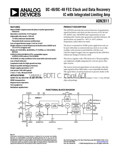
The ADN2811 is a clock and data recovery IC designed for SONET OC‑48 and OC‑48 FEC rates. It integrates a quantizer, loss‑of‑signal detector, and PLL, supporting selectable reference clocks from 19.44 MHz to 155.52 MHz and LVPECL/LVDS/LVCMOS/LVTTL compatible inputs. The device operates from a single 3.3 V supply and consumes about 540 mW.
The datasheet includes detailed electrical specifications, absolute maximum ratings, thermal characteristics, pin configuration, functional block diagrams, and ordering information. It also provides design guidelines for PCB layout, input sensitivity, jitter performance, and test modes such as loopback and bypass.
| Input Voltage Range @ PIN or NIN (DC‑Coupled) | 0 V to 1.2 V |
|---|---|
| Upper -3 dB Bandwidth | 19 GHz |
| Power Supply Voltage | 3.0 V to 3.6 V |
| Power Supply Current | 150 mA to 215 mA |
| Single‑Ended Output Swing (Vse) | 300 mV to 600 mV |
| Maximum Junction Temperature | 165 °C |
| Package Size | 7 mm × 7 mm, 48‑lead LFCSP |
The device accepts a DC‑coupled input voltage from 0 V to 1.2 V on the PIN or NIN pins.
It operates from a single supply of 3.0 V to 3.6 V.
The chip is housed in a 7 mm × 7 mm, 48‑lead LFCSP package.
The maximum junction temperature is rated at 165 °C.