
ADN2865 is a clock and data recovery IC that supports 12.3Mb/s to 2.7Gb/s continuous rate and has a built-in loop-timed SERDES.
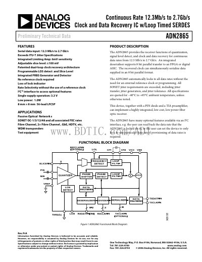
The ADN2865 provides continuous‑rate clock and data recovery for serial data streams from 12.3 Mb/s up to 2.7 Gb/s. It integrates a limiting amplifier, programmable loss‑of‑signal detection, and a PRBS generator/detector, and operates from a single 3.3 V supply without an external reference clock.
The device is offered in an 8 mm × 8 mm 56‑lead LFCSP package and includes a PC™ interface for configuration and status read‑back. Detailed specifications cover input voltage ranges, jitter performance, output swing for CML and LVDS, and absolute maximum ratings.
| Data Rate | 12.3 Mb/s – 2.7 Gb/s |
|---|---|
| Power Supply Voltage | 3.0 V – 3.6 V |
| Operating Temperature Range | -40 °C to +85 °C |
| Input Voltage Range (dc‑coupled) | 1.8 V – 2.8 V |
| Typical Power Consumption | 1.0 W |
No, the device operates without a reference clock.
It includes a loss‑of‑lock indicator.
The device is supplied in an 8 mm × 8 mm 56‑lead LFCSP package.
The typical power consumption is about 1.0 W.