
ADN2813 is a Clock and Data Recovery IC with Integrated Limiting Amp that supports continuous rate of 10 Mb/s to 1.25 Gb/s. It exceeds SONET requirements for jitter transfer/generation/tolerance and features adjustable quantizer sensitivity, adjustable slice level, and no reference clock requirement.
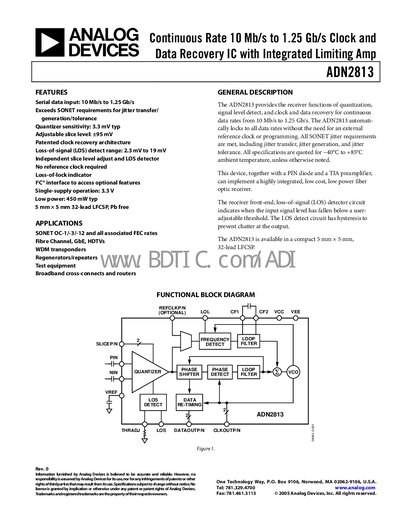
The ADN2813 is a continuous‑rate clock and data recovery IC that operates from 10 Mb/s to 1.25 Gb/s without requiring an external reference clock. It meets SONET jitter requirements and provides loss‑of‑signal detection, loss‑of‑lock indication, and a PC interface for optional features.
The device is offered in a compact 5 mm × 5 mm 32‑lead LFCSP package, operates from a single 3.3 V supply with typical power consumption of 450 mW, and includes detailed pin descriptions, timing diagrams, and electrical characteristics for designers of fiber‑optic receivers, regenerators, and high‑speed data equipment.
| Data Rate | 10 Mb/s to 1.25 Gb/s |
|---|---|
| Power Supply Voltage | 3.0 V – 3.6 V |
| Power Supply Current (locked to 1.25 Gb/s) | 139 mA typ, 155 mA max |
| Input Voltage Range (PIN/NIN, dc‑coupled) | 1.8 V min – 2.8 V max |
| Jitter Transfer Bandwidth (OC‑12) | 75 kHz – 130 kHz |
The ADN2813 supports continuous data rates from 10 Mb/s up to 1.25 Gb/s.
No, the device automatically locks to all data rates without an external reference clock.
Typical power consumption is 450 mW.
It is available in a 5 mm × 5 mm 32‑lead LFCSP package.