
The ADN2816 is a clock and data recovery IC from Analog Devices that provides 10 Mb/s to 675 Mb/s of continuous data rates. The IC has a patented clock recovery architecture, does not require a reference clock, and has a loss-of-lock indicator. The ADN2816 also has an I2C interface to access optional features.
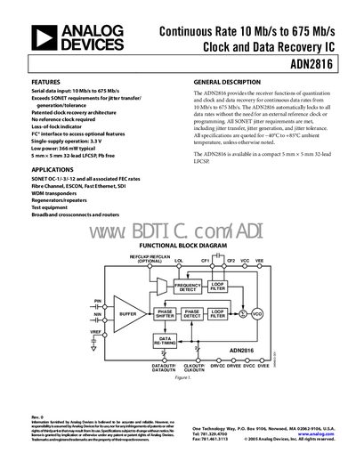
The ADN2816 is a clock and data recovery IC that receives and recovers continuous data rates from 10 Mb/s to 675 Mb/s. It automatically locks to any data rate without an external reference clock and includes features such as loss‑of‑lock indication, low power operation, and a 3.3 V single‑supply.
The device is offered in a 5 mm × 5 mm 32‑lead LFCSP package and is suited for SONET, Fibre Channel, Fast Ethernet, and other high‑speed communication applications. Key specifications include a typical power consumption of 366 mW, operating temperature range of –40 °C to +85 °C, and LVDS output levels suitable for high‑speed signaling.
| Data Rate | 10 Mb/s to 675 Mb/s |
|---|---|
| Supply Voltage | 3.0 V to 3.6 V |
| Typical Power Consumption | 366 mW |
| Operating Temperature Range | -40 °C to +85 °C |
| Input Voltage Range | 1.8 V to 2.8 V |
| LVDS Output High Voltage | 1475 mV (at 655 Mb/s) |
No, the ADN2816 automatically locks to all data rates without the need for an external reference clock.
Pin 16 (LOL) is the loss‑of‑lock indicator and is LVTTL active high.
The typical power consumption is 366 mW.