
ADN2819 is a clock and data recovery IC with integrated limiting amp produced by Analog Devices
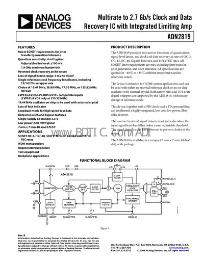
The ADN2819 is a multirate clock and data recovery IC that meets SONET jitter requirements and supports rates up to OC‑48, Gigabit Ethernet, and 15/14 FEC. It offers adjustable slice level, loss‑of‑signal detection, loopback test mode, and single‑supply operation at 3.3 V.
The datasheet provides full electrical specifications, absolute maximum ratings, pin descriptions, functional block diagrams, and design guidelines for PCB layout and AC‑coupling. It also includes jitter performance data, loss‑of‑lock detector characteristics, and ordering information.
| Quantizer sensitivity | 4 mV typical |
|---|---|
| Single‑supply operation voltage | 3.3 V |
| Typical power consumption | 540 mW |
| Package | 7 mm × 7 mm 48‑lead LFCSP |
| Input voltage range (PIN/NIN) | 0 V – 1.2 V |
| Upper –3 dB bandwidth | 19 GHz |
| Supply voltage rating | 3.0 V – 3.6 V |
| Supply current | 150 mA – 215 mA |
The ADN2819 accepts a dc‑coupled input voltage from 0 V to 1.2 V on the PIN or NIN pins.
Typical power consumption is 540 mW.
Yes, it operates from a single 3.3 V supply.