
The ADN2815 is a Clock and Data Recovery IC that supports continuous data rates from 10 Mb/s to 1.25 Gb/s. It exceeds SONET requirements for jitter transfer/generation/tolerance and does not require an external reference clock.
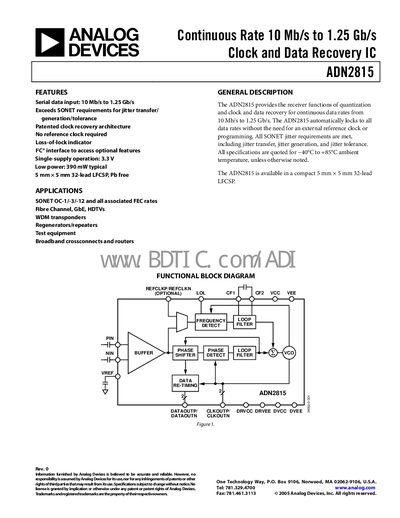
The ADN2815 is a clock and data recovery IC that operates over continuous data rates from 10 Mb/s to 1.25 Gb/s. It automatically locks to any data rate without requiring an external reference clock and meets SONET jitter requirements.
The document includes detailed electrical specifications, pin descriptions, timing diagrams, jitter performance, absolute maximum ratings, and ordering information for the 5 mm × 5 mm 32‑lead LFCSP package.
| Data Rate | 10 Mb/s to 1.25 Gb/s |
|---|---|
| Power Supply Voltage | 3.0 V to 3.6 V |
| Power Supply Current (locked to 1.25 Gb/s) | 118 mA to 131 mA |
| Operating Temperature Range | -40 °C to +85 °C |
| Package | 5 mm × 5 mm 32‑lead LFCSP |
No, the device automatically locks to all data rates without the need for an external reference clock.
The device operates from a 3.0 V to 3.6 V supply.
It operates from –40 °C up to +85 °C.