
This document provides information about the PCB board layout for the SOT810-1 package, suitable for reflow soldering. It includes dimensions for solder lands, solder paste clearance, and occupied area.
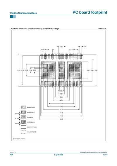
This document supplies the PCB footprint information required for reflow soldering of the Philips SOT810-1 (HSSON18) semiconductor package. It lists the key geometric parameters and recommended soldering tolerances.
Key dimensions include solder land size, solder resist area, clearance, and solder paste thickness, all expressed in millimetres. The data are intended for designers creating printed‑circuit‑board layouts for this component.
| Solder land dimension | 7.80 mm |
|---|---|
| Solder resist dimension | 11.40 mm |
| Clearance dimension | 12.30 mm |
| Solder paste thickness | 0.050 mm |
The solder land dimension is 7.80 mm.
A clearance of 12.30 mm is specified.
The document specifies a solder paste thickness of 0.050 mm.
The solder resist dimension is 11.40 mm.