
The XC6209/XC6212 series are highly precise, low noise, positive voltage LDO regulators manufactured using CMOS processes. The series achieves high ripple rejection and low dropout and consists of a voltage reference, an error amplifier, a current limiter and a phase compensation circuit plus a driver transistor. Output voltage is selectable in 50mV increments within a range of 0.9V ~ 6.0V. The series is also compatible with low ESR ceramic capacitors which give added output stability. This stability can be maintained even during load fluctuations due to the excellent transient response of the series. The current limiter's foldback circuit also operates as a short protect for the output current limiter and the output pin. The CE function enables the output to be turned off, resulting in greatly reduced power consumption.
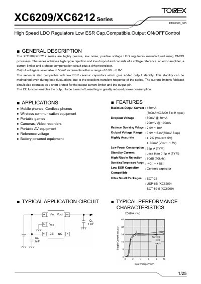
The XC6209/XC6212 series are high‑precision, low‑noise LDO regulators manufactured with CMOS technology. They offer selectable output voltages from 0.9 V to 6.0 V in 50 mV steps, high ripple rejection, low dropout, and a CE pin for output shutdown to save power.
The document provides detailed electrical characteristics, pin configurations for SOT‑25, SOT‑89‑5 and USP‑6B packages, recommended capacitor usage, marking conventions, and ordering information for designers and service engineers.
| Output Voltage Range | 0.9 V ~ 6.0 V (50 mV steps) |
|---|---|
| Dropout Voltage (30 mA) | 60 mV typical |
| Ripple Rejection (10 kHz) | 70 dB |
| Package Types | SOT‑25, SOT‑89‑5, USP‑6B |
The output voltage can be set from 0.9 V to 6.0 V in 50 mV increments.
The series is compatible with low‑ESR ceramic capacitors, which improve output stability.
The CE pin enables the output to be turned off, greatly reducing power consumption.