
SSM3J01F is a P-channel MOS type field effect transistor produced by Toshiba. It is suitable for high speed switching applications. The transistor has small package, low on resistance, low gate threshold voltage and other features.
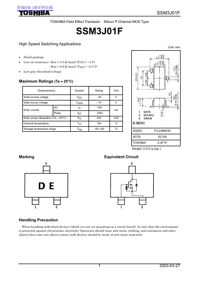
This document is a technical datasheet for the Toshiba SSM3J01T, a Silicon P-Channel MOS Type Power Management Switch. It highlights features such as high-speed switching applications, low on-resistance (Ron max 0.4 Ω at Vgs = -4V), and a small package size.
The document provides comprehensive electrical characteristics including gate leakage current, breakdown voltage, threshold voltage, and capacitance values measured at Ta = 25°C. It also includes graphical data for drain-source on-resistance versus temperature and safe operating area curves.
| Drain-Source Voltage (Vds) | -30 V |
|---|---|
| Gate-Source Voltage (Vgs) | +10 V |
| Drain Current (DC ID) | 1.7 A |
| Pulse Drain Current (Ipp) | 34 A |
| Drain Power Dissipation | 1250 mW |
| Channel Temperature (Tch) | 150 °C |
| Storage Temperature Range | -55~150 °C |
| Drain-Source ON Resistance (Vgs = -4V) | 0.4 Ω max |
| Gate Threshold Voltage (Vth) | 0.6 to -1.1 V |
| Input Capacitance (Ciss) | 240 pF typ. |
The document recommends a gate-source voltage of -2.5 V or higher to turn on this product.
The device has a maximum drain-source voltage rating of -30 V and a maximum gate-source voltage rating of +10 V.
The typical weight for handling individual devices is 10 mg.
A maximum drain power dissipation of 1250 mW is specified when mounted on an FR4 board measuring 25.4 mm x 25.4 mm.