
This document describes the features and characteristics of the SSM3J09FU model, including small package, low on resistance, and high-speed switching applications.
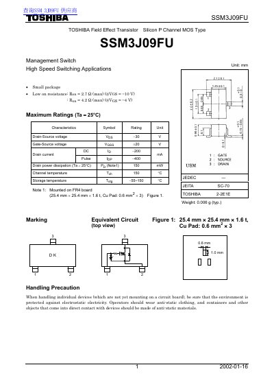
This document is a technical datasheet for the Toshiba SSM3J09FU, a silicon P-Channel Field Effect Transistor (MOSFET). The device features a small package and is optimized for high-speed switching applications with a maximum drain-source voltage of 30V.
| Drain-Source voltage (Vds) | -30 V |
|---|---|
| Gate-Source voltage (Vgs) | +20 V |
| Drain current (DC Id) | -200 mA |
| Drain power dissipation (Ta = 25°C) | 150 mW |
| Channel temperature (Tch) | 150 °C |
| Storage temperature (Tstg) | -55~150 °C |
The datasheet recommends a voltage of -4.0 V or higher.
Operators should wear anti-static clothing and use containers made of anti-static materials.