
This document describes the features and characteristics of the SSM3J02T power management switch, a silicon P-channel MOS type field effect transistor. It is suitable for high-density mounting and offers low ON resistance and low-voltage operation. The document also provides the maximum ratings for this model, including drain-source voltage, gate-source voltage, and drain current.
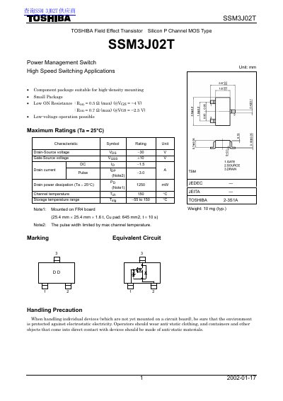
This document is a technical datasheet for the TOSHIBA SSM3J02T, a Silicon P Channel MOS Type Power Management Switch. It highlights features such as high-speed switching applications, low ON resistance (Ron max 0.7 Ω), and suitability for high-density mounting in small packages.
The text provides comprehensive electrical specifications including maximum ratings like a drain-source voltage of -30 V and a pulse current of 30 A. Detailed graphs illustrate the relationship between ambient temperature, drain current, and on-resistance, along with safe operating area curves.
| Pulse Current (IPP) | 30 A |
|---|---|
| Drain Power Dissipation (Ta = 25°C) | 1250 mW |
| Channel Temperature (Tch) | 150 °C |
| Gate Threshold Voltage (Vth) Max | -1.1 V |
| Drain-Source ON Resistance (Ron) Max @Vgs=-2.5V | 0.7 Ω |
| Input Capacitance (Ciss) | 150 pF |
The document recommends a gate-source voltage of -2.5 V or higher.