
SSM3J02F is a high-performance field-effect transistor produced by TOSHIBA, with small package, low switching resistance, and low gate threshold voltage
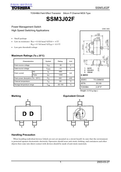
This document is a technical datasheet for the Toshiba SSM3J02F, a Field Effect Transistor (MOSFET) designed as a Silicon P-Channel device. It is intended for high-speed switching applications in power management circuits.
The datasheet provides comprehensive electrical characteristics including maximum ratings, threshold voltage, on-resistance, and capacitance values at 25°C. It also includes graphical data such as the Safe Operating Area (SOA), drain-source ON resistance versus temperature curves, and switching time test circuit diagrams.
| Gate-source voltage (VGSS) | +10 V |
|---|---|
| Pulse Drain current (IDP) | -1200 mA |
| Drain power dissipation | 200 mW |
| Channel temperature (Tch) | 150 °C |
| Storage temperature range | -55 ~ 150 °C |
| Gate threshold voltage (Vth) | -0.6 V to -1.1 V |
| Drain-source ON resistance (RDS(ON)) | Max 0.7 Ω @ VGS=-2.5V |
The datasheet recommends a voltage of -2.5 V or higher to turn on this product.
The device can handle a DC drain current of up to 600 A.
The maximum drain power dissipation is rated at 200 mW.
A gate-source voltage of -2.5 V or higher is recommended for switching operation.