
The CDCLVP110 is a low-voltage 1:10 LVPECL/HSTL with selectable input clock driver. It distributes one differential clock input pair (CLK0, CLK1) to ten pairs of differential LVPECL clock outputs (Q0, Q9) with minimum skew for clock distribution. The CDCLVP110 can accept two clock sources to an input multiplexer. The CLK0 input accepts either LVECL/LVPECL input signals, while CLK1 accepts an HSTL input signal when operated under LVPECL conditions. The CDCLVP110 is specifically designed for driving 50-Ω transmission lines. If single-ended input operation is required, the VBB reference voltage output is used. In this case, the VBB pin should be connected to CLK0 and bypassed to GND via a 10-nF capacitor.
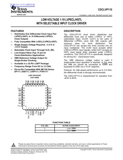
The CDCLVP110 is a clock driver designed for distribution applications requiring low output skew. It accepts a single differential clock input pair from either LVPECL or HSTL standards and distributes it to ten pairs of differential LVPECL clock outputs (Q0 through Q9). The device supports selectable input clock sources via the CLK_SEL pin, allowing the user to choose between the CLK0 and CLK1 input pairs.
| Frequency Range | DC to 3.5 GHz |
|---|---|
| Operating Temperature | -40 °C to 85 °C |
| Supply Voltage (LVPECL) | 2.375 V to 3.8 V |
| Supply Voltage (HSTL) | 2.375 V to 3.8 V |
| Output Skew (Typical) | 15 ps |
| Package Type | 32-Pin LQFP |
The device functions up to a maximum frequency of 3.5 GHz.
The device functions up to a maximum frequency of 3.5 GHz.
The device requires a single supply voltage between 2.375 V and 3.8 V.
The typical output-to-output skew is 15 ps.