
The CDCM1802 is a clock buffer with a programmable divider, LVPECL I/O and additional LVCMOS output. It distributes one differential clock input to one LVPECL differential clock output and one LVCMOS single-ended output. The programmable output divider is suitable for LVPECL and LVCMOS outputs. The 1.6-ns output skew between LVCMOS and LVPECL transitions minimizes noise. The device operates at a supply voltage of 3.3 V (2.5 V functional) and has a signaling rate of up to 800 MHz LVPECL and 200 MHz LVCMOS. The differential input stage has a wide common-mode range and also provides a VBB bias voltage output for single-ended input signals. The receiver input threshold is ±75 mV. The device is packaged in a 16-pin QFN package (3 mm x 3 mm).
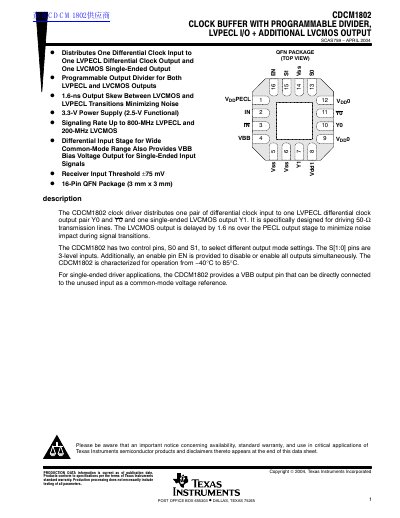
The CDCM1802 is a clock buffer designed to distribute one differential clock input to one LVPECL differential clock output and one single-ended LVCMOS output. It features a programmable output divider for both output types and includes a 1.6-ns output skew between LVCMOS and LVPECL transitions to minimize noise. The device supports signaling rates up to 800-MHz for LVPECL and 200-MHz for LVCMOS.
| Supply Voltage | 3 V to 3.6 V |
|---|---|
| Operating Temperature | -40°C to 85°C |
| LVPECL Input Frequency | 0 to 800 MHz |
| Package Type | 16-Pin QFN |
| Output Skew (LVCMOS to LVPECL) | 1.6 ns |
The device supports an input frequency up to 800 MHz.
The CDCM1802 is characterized for operation from −40°C to 85 °C.
The output skew between LVCMOS and LVPECL transitions is 1.6 ns.