
The product is a clock buffer that supports 1:3 LVPECL clock output and programmable divider. It features low output skew, wide common mode range, differential input stage and single-ended input signal VBB bias voltage output.
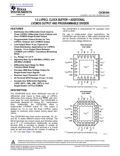
The Texas Instruments CDCM1804 is a clock driver designed to distribute a single pair of differential clock inputs to three pairs of LVPECL differential outputs (Y[2:0]) and one single-ended LVCMOS output (Y3). It features a programmable output divider for the LVPECL and LVCMOS channels, allowing frequency division based on control terminal settings.
The device operates with a supply voltage range of 3 V to 3.6 V and supports signaling rates up to 800 MHz for LVPECL outputs and 200 MHz for the LVCMOS output. It includes features such as low output skew, a wide common-mode input range accepting various differential signaling standards (LVDS, HSTL, CML), and a dedicated VBB bias voltage output for single-ended inputs.
| Supply Voltage Range | 3 V - 3.6 V |
|---|---|
| LVPECL Signaling Rate | Up to 800-MHz |
| LVCMOS Signaling Rate | 200-MHz |
| Package Type | 24-Terminal QFN Package (4mm x 4mm) |
The CDCM1804 supports a signaling rate of up to 800-MHz for LVPECL outputs.
The typical low-output skew for the LVPECL outputs is 15 ps.