
The document describes a phase-locked loop clock driver for double data-rate synchronous DRAM applications. It features spread spectrum clock compatibility, operating frequency range of 60 to 140 MHz, low jitter, and the capability to distribute one differential clock input to ten differential outputs. It also includes a two-line serial interface, high-impedance state, and low quiescent current consumption.
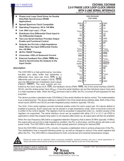
The CDCV850 is a high-performance, low-skew, low-jitter zero delay buffer designed to distribute a differential clock input pair to ten differential pairs of clock outputs and one differential pair of feedback clock outputs. It features a 2-line serial interface for controlling individual output enable states and supports spread spectrum clocking for reduced EMI. The device operates with a supply voltage of 2.5 V and is available in a 48-pin TSSOP package.
| Operating Frequency | 60 to 140 MHz |
|---|---|
| Low Jitter (cyc-cyc) | +/- 75 ps |
| Supply Voltage (AVDD) | 2.5 V (nom) |
| Package Type | 48-pin TSSOP |
| Clock Frequency Range | 60 to 140 MHz |
The stabilization time required for the integrated PLL circuit to obtain phase lock is 10 us.
Yes, the CDCV850 is able to track spread spectrum clocking for reduced EMI.