
This file is the scas727b manual for the cdcp1803 clock driver
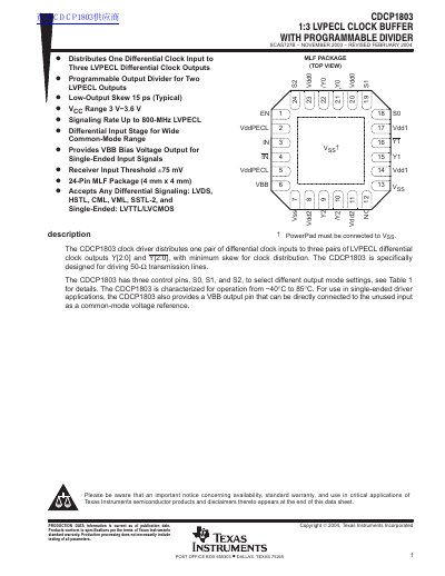
The CDCP1803 is a differential clock driver designed to distribute one pair of differential clock inputs to three pairs of LVPECL differential clock outputs. It features a programmable output divider for two of the outputs, allowing for flexible frequency division ratios.
The device accepts various differential signaling standards including LVDS, HSTL, CML, and VML, as well as single-ended LVTTL/LVCMOS signals via a bias voltage output (VBB). It is characterized for operation over an industrial temperature range of -40°C to 85°C and is packaged in a 24-pin MLF format.
| Operating Temperature Range | -40°C to 85°C |
|---|---|
| Maximum Input Frequency | 800 MHz |
| Output Skew (Typical) | 15 ps |
| Package Type | 24-Pin MLF Package (4 mm x 4mm) |
The device accepts LVDS, HSTL, CML, VML, SSTL-2, and single-ended LVTTL/LVCMOS signals.
The CDCP1803 has three control pins (S0, S1, and S2) to select different output mode settings.