
CDCV857 is a 2.5V phase-locked loop (PLL) clock driver from TI, which is used for double data rate synchronous DRAM applications. The device adopts low-power design, and has low jitter, low skew, zero delay and other characteristics. Its working frequency range is 60MHz to 200MHz, and it can drive 10 differential clock outputs. When the input clock frequency is lower than 20MHz, the device will enter low power mode, and shut down the PLL.
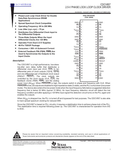
The CDCV857 is a high-performance, low-skew, zero delay buffer designed for double data rate synchronous DRAM applications. It operates from dual 2.5-V supplies and features an integrated phase-locked loop (PLL) circuitry to distribute one differential clock input pair to ten differential output pairs, along with one feedback output pair.
The device supports spread spectrum clocking compatibility to reduce electromagnetic interference (EMI). When the power-down pin is high, outputs switch in phase and frequency with the input clock. When low, all outputs enter a high-impedance state, shutting down the PLL for low-power operation. The chip operates over an industrial temperature range of 0°C to 85°C.
| Operating Frequency | 60 to 200 MHz |
|---|---|
| Low Jitter (cycle-to-cycle) | +/-75 ps |
| Supply Voltage | 2.3 V to 2.7 V |
| Operating Temperature Range | 0°C to 85°C |
| Package Type | 48-Pin TSSOP |
| Quiescent Current (typical) | < 200 µA |
The stabilization time required following power up in PLL mode is 10 µs.
Yes, the device is able to track spread spectrum clocking for reduced EMI.
When PWRDWN is low, all outputs are disabled to a high impedance state (3-state), and the PLL is shut down.