
The CDCV855 is a high-performance, low-skew, low-jitter zero delay buffer that distributes a differential clock input pair (CLK, CLK) to four differential pairs of clock outputs (Y[0:3], Y[0:3]) and one differential pair of feedback clock outputs (FBOUT, FBOUT). When PWRDWN is high, the outputs switch in phase and frequency with CLK. When PWRDWN is low, all outputs are disabled to a high-impedance state (3-state), and the PLL is shut down (low-power mode). The device also enters this low-power mode when the input frequency falls below a suggested detection frequency that is below 20 MHz (typical 10 MHz). An input frequency detection circuit detects the low-frequency condition and after applying a >20-MHz input signal this detection circuit turns on the PLL again.
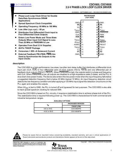
The CDCV855 is a high-performance, low-skew, zero delay buffer designed to distribute a differential clock input pair to four differential pairs of clock outputs and one feedback output. It operates from dual 2.5-V supplies with an operating frequency range of 60 MHz to 180 MHz.
| Operating Frequency | 60 MHz to 180 MHz |
|---|---|
| Supply Voltage | 2.5 V (nominal) |
| Package Type | 28-Pin TSSOP |
| Quiescent Current | < 200 µA |
| Jitter (cycle-to-cycle) | +50 ps Vpp |
When PWRDWN is low, all outputs are disabled to a high-impedance state and the PLL is shut down.
The device operates with an input clock frequency ranging from 60 MHz to 180 MHz.
The device consumes less than 200 µA of quiescent current.