
SCAS688A is a 1.8V phase-locked loop clock driver for double data rate (DDR II) applications. It is spread spectrum clock compatible and operates at a frequency range of 10 MHz to 400 MHz. It has features such as low current consumption, low jitter, low output skew, and low phase offset. It distributes one differential clock input to ten differential outputs.
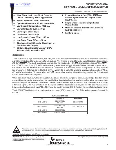
The CDCU877 is a Zero-delay buffer designed to distribute a differential clock input pair to ten differential pairs of clock outputs and one feedback output. It features low jitter and skew specifications suitable for Double Data Rate (DDR II) applications.
The device operates from an operating frequency range of 10 MHz to 400 MHz and supports spread spectrum clocking (SSC). It is available in a 52-ball BGA package or a 40-pin MLF package.
| Low Jitter (Cycle-Cycle) | +30 ps |
|---|---|
| Low Output Skew | 35 ps |
| Operating Temperature Range | -40°C to 85°C |
| Output Distribution | Ten differential outputs |
Yes, the device is able to track spread spectrum clocking (SSC) for reduced EMI.
When AVpp is grounded, the PLL is turned off and bypassed for test purposes.