
Texas Instruments CDCLVD110 Programmable Low-Voltage 1:10 LVDS Clock Driver Datasheet

The CDCLVD110 is a programmable low-voltage 1:10 LVDS clock driver. It features low-output skew, distribution of one pair of differential clock inputs to 10 pairs of differential clock outputs, VCC range of 2.5V, and a typical signaling rate capability of up to 1.1 GHz.
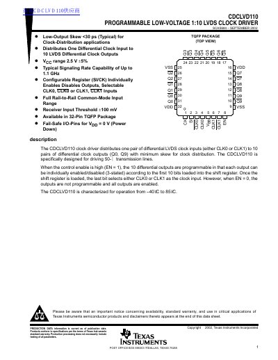

Texas Instruments CDCLVD110 Programmable Low-Voltage 1:10 LVDS Clock Driver Datasheet - cover page
Brand
Texas Instruments
Category
Other Electronics
Document type
Datasheet
Language
English
Pages
10
File format
PDF
File size
134 KB
Published
01 August, 2012
Updated
28 September, 2023
MD5 checksum
414545E46B6240A6A7ACCF8BEF686737

About this manual

The CDCLVD110 is a programmable low-voltage 1:10 LVDS clock driver designed for clock distribution applications. It distributes one pair of differential LVDS clock inputs to 10 pairs of differential clock outputs with minimum skew, specifically for driving 50-Ω transmission lines. The device is available in a 32-pin TQFP package.

What's inside

  • Terminal Functions
  • Absolute Maximum Ratings
  • Recommended Operating Conditions
  • Driver Electrical Characteristics
  • Receiver Electrical Characteristics
  • Supply Current Characteristics
  • LVDS Switching Characteristics
  • Control Register Characteristics
  • Specification of Control Register
  • Application Information

Specifications

Operating Temperature-40°C to 85°C
Output Skew< 30 ps (Typical)
Package32-Pin TQFP

Frequently asked questions

What is the typical output skew of the CDCLVD110?

The typical output skew is less than 30 ps.

What is the maximum operating temperature for this device?

The CDCLVD110 is characterized for operation from -40°C to 85°C.

Download PDF (134 KB)

More Texas Instruments Manuals


View all Texas Instruments manuals →