
the cdcf5801 is a low-jitter clock multiplier that can multiply the input clock frequency by 1, 2, 4, or 8 times. The output frequency range is 25 mhz to 280 mhz, and the input frequency range is 12.5 mhz to 240 mhz. It has single-ended input and differential output, and can drive lvpecl, lvds, and lvttl.
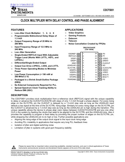
The CDCF5801 is a clock multiplier that provides frequency multiplication from a reference clock (REFCLK) signal. It features unique capability to delay or advance the output clocks (CLKOUT/CLKOUTB) with steps of only 1.3 mUI through an integrated phase aligner, allowing for precise phase alignment between system clocks.
The device supports input frequencies ranging from 12.5 MHz to 240 MHz and generates output frequencies from 25 MHz to 280 MHz using pre-divider and post-divider pins. It offers various power-down modes, low power consumption under 190 mW at 3.3 V, and is packaged in a Shrink Small-Outline Package (DBQ) requiring no external components for the PLL.
| Low-Jitter Clock Multiplier Ratios | x1, x2, x4, x8 |
|---|---|
| Programmable Delay Step Size | 1.3 mUI |
| Output Frequency Range | 25 MHz to 280 MHz |
| Input Frequency Range | 12.5 MHz to 240 MHz |
| Operating Temperature Range | -40°C to 85°C |
No, no external components are required for the PLL to function.
Yes, the outputs can drive LVPECL, LVDS, and LVTTL signals.