
The CDC339 is a high-performance, low-skew clock driver specifically designed for applications requiring synchronized output signals at both the primary clock frequency and one-half the primary clock frequency. It features low output skew and low pulse skew, TTL-compatible inputs and outputs, distributes one clock input to eight outputs (four same-frequency outputs and four half-frequency outputs), distributed VCC and ground pins to reduce switching noise, high-drive outputs, state-of-the-art EPIC-IIIB BiCMOS design to reduce power dissipation, and multiple package options.
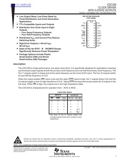
The CDC339 is a high-performance, low-skew clock driver specifically designed for applications requiring synchronized output signals at both the primary clock frequency and one-half the primary clock frequency. It features four Y outputs that switch in phase with the clock input and four Q outputs that toggle at half the clock frequency. The device includes an output-enable (OE) input and a clear (CLR) input to control output states and asynchronous reset functionality.
| Operating Temperature | -40°C to 85°C |
|---|---|
| Clock Frequency | 80 MHz |
| High-Level Output Current | -48 mA |
| Low-Level Output Current | 48 mA |
| Package Options | DB and DW |
The four Y outputs switch at the same frequency as the clock input, while the four Q outputs switch at one-half the frequency of the clock.
Taking the clear (CLR) input low asynchronously resets the Q outputs to the low level.
When the output-enable (OE) input is high, the outputs are in the high-impedance state.