
The CDC351 is a high-performance clock driver circuit from Texas Instruments that distributes one input clock signal to 10 output clock signals with minimum skew. The CDC351 operates at 3.3 V VCC, and has high drive current and low power consumption.
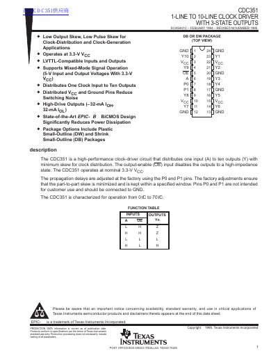
The CDC351 is a high-performance clock-driver circuit designed to distribute a single clock input signal to ten separate outputs (Y0-Y9) while minimizing skew. It features state-of-the-art EP/C-IIB BiCMOS design for reduced power dissipation and operates at a nominal 3.3V supply voltage. The device supports mixed-mode signal operation, allowing 5-V inputs and outputs with a 3.3-V output-enable (OE) input.
The chip includes factory-adjusted propagation delays to ensure minimal part-to-part skew, keeping it within a specified window. It offers high-drive outputs capable of sourcing or sinking up to 32 mA. The CDC351 is available in Plastic Small-Outline (DW) and Shrink Small-Outline (DB) packages and is characterized for operation over an operating free-air temperature range of 0°C to 70°C.
| Supply Voltage (VCC) | 3 V to 3.6 V |
|---|---|
| Operating Temperature Range | 0°C to 70°C |
| Input Clock Frequency (fclk) | 100 MHz |
| High-Level Output Current (IOH) | -32 mA |
| Low-Level Output Current (IOL) | 32 mA |
| Package Options | DW, DB |
The input clock frequency can be up to 100 MHz.
It distributes one input signal to ten outputs (Y0 through Y9).