
The CDC536 is a high-performance, low-skew, low-jitter clock driver. It uses a phase-lock loop (PLL) to precisely align, in both frequency and phase, the clock output signals to the clock input (CLKIN) signal. It is specifically designed for use with synchronous DRAMs and popular microprocessors operating at speeds from 50 MHz to 100 MHz or down to 25 MHz on outputs configured as half-frequency outputs. The CDC536 operates at 3.3-V VCC and is designed to drive a 50-Ω transmission line. The feedback input (FBIN) is used to synchronize the output clocks.
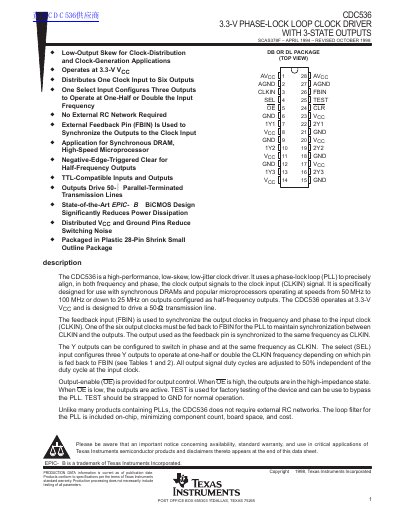
The CDC536 is a high-performance, low-skew, low-jitter clock driver that uses a phase-lock loop (PLL) to align clock output signals to the input clock signal in both frequency and phase. It operates at 3.3 V and is specifically designed for use with synchronous DRAMs and microprocessors operating at speeds from 50 MHz to 100 MHz, or down to 25 MHz on half-frequency outputs. The device distributes one clock input to six outputs and can configure three of these outputs to operate at one-half or double the input frequency based on the SEL input and feedback configuration. Unlike many other PLL products, the CDC536 does not require external RC networks as the loop filter is included on-chip.
| Supply Voltage | 3 V to 3.6 V |
|---|---|
| High-Level Output Current | -32 mA |
| Low-Level Output Current | 32 mA |
| Input Frequency Range (Config A) | 50 MHz to 100 MHz |
| Input Frequency Range (Config B) | 25 MHz to 50 MHz |
No, the CDC536 does not require external RC networks because the loop filter for the PLL is included on-chip.
The CDC536 operates at 3.3 V.
The CDC536 distributes one clock input to six outputs.