
The CDC340 is a high-performance clock driver circuit that distributes one (A) input signal to eight (Y) outputs with minimum skew for clock distribution. Through the use of the control pins (1G and 2G), the outputs can be placed in a high state regardless of the A input. The propagation delays are adjusted at the factory using the P0 and P1 pins. These pins are not intended for customer use and should be strapped to GND. The CDC340 is characterized for operation from 0°C to 70°C.
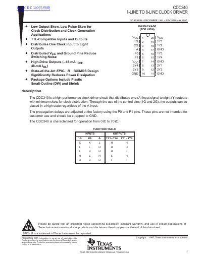
The CDC340 is a high-performance clock-driver circuit designed to distribute a single input signal (A) to eight outputs (Y) while maintaining minimum skew. It features TTL-compatible inputs and outputs, distributed Vcc and ground pins to reduce switching noise, and high-drive outputs capable of sourcing or sinking 48 mA. The device utilizes an EPIC-IIB BiCMOS design to significantly reduce power dissipation.
| Operating temperature range | 0°C to 70°C |
|---|---|
| High-level output current (IOH) | -48 mA |
| Low-level output current (IOL) | 48 mA |
The recommended operating conditions specify a maximum supply voltage of 5.25 V.
Each output is rated to sink up to 48 mA when in the low state.