
The CDC509 is a high-performance, low-jitter, low-skew phase-lock loop (PLL) clock driver from Cypress Semiconductor. It uses a PLL to precisely align the feedback (FBOUT) output to the clock (CLK) input signal, both in frequency and phase. It is specifically designed for use with synchronous DRAMs. The CDC509 operates at 3.3 V VCC and is designed to drive up to five clock loads per output. One bank of five outputs and one bank of four outputs provide nine low-skew, low-jitter copies of CLK. Output signal duty cycles are adjusted to 50 percent, independent of the duty cycle at CLK. Each bank of outputs can be enabled or disabled separately via the control (1G and 2G) inputs. When the G inputs are high, the outputs switch in phase and frequency with CLK; when the G inputs are low, the outputs are disabled to the logic-low state. Unlike many products containing PLLs, the CDC509 does not require external RC networks. The PLL's loop filter is integrated on-chip, reducing PCB area.
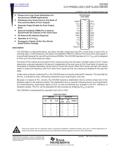
The CDC509 is a phase-lock loop (PLL) clock driver designed to distribute one clock input to multiple outputs with low skew and jitter. It uses an internal PLL to align the feedback output frequency and phase precisely with the clock input, specifically for use with synchronous DRAMs.
The device operates at 3.3V and is available in a 24-pin plastic thin-shrink small-outline package (PW). Unlike many other PLL products, the CDC509 does not require external RC networks as its loop filter is included on-chip. It features two separate output banks: one with five outputs and another with four outputs, each controlled by independent enable inputs.
| Operating Temperature Range | 0°C to 70°C |
|---|---|
| Clock Frequency Range | 25 MHz to 125 MHz |
| Stabilization Time | 11 ms |
| Package Type | 24-Pin Thin Shrink Small-Outline Package (PW) |
No, the loop filter for the PLL is included on-chip.
The device requires a stabilization time of 11 ms to achieve phase lock.
Yes, by strapping AVcc to ground.