
CDC857-2 and CDC857-3 are 2.5-/3.3-V phase-lock loop clock drivers for Double Data Rate Synchronous DRAM applications. It distributes one differential clock input to ten differential outputs. External feedback pins (FBIN, FBIN) are used to synchronize the outputs to the clock input. It operates at VCC = 2.5 V and AVCC = 3.3 V. And it is packaged in plastic 48-pin (DGG) thin shrink small-outline package (TSSOP).
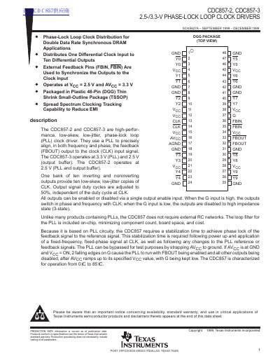
The CDC857-2 and CDC857-3 are high-performance, low-skew, low-jitter phase-lock loop (PLL) clock drivers designed to distribute one differential clock input to ten differential outputs. These devices use an integrated PLL to precisely align the feedback output to the clock input in both frequency and phase, operating at supply voltages of 2.5 V (CDC857-2) or 3.3 V (CDC857-3).
| Operating temperature range | 0°C to 85°C |
|---|
No, the loop filter for the PLL is included on-chip, minimizing component count.
The CDC857 is characterized for operation from 0°C to 85°C.