
cdc2509b 3.3-v phase-lock loop clock driver is a phase-lock loop clock distributor for synchronous dram applications. it distributes one clock input to one bank of five and one bank of four outputs. each output bank has a separate output enable. the external feedback (fbin) terminal is used to synchronize the outputs to the clock input. cdc2509b operates at 3.3-v vcc. it also provides integrated series damping resistors, making it ideal for driving point-to-point loads.
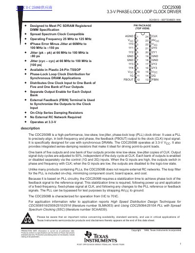
The CDC2509B is a high-performance, low-skew, low-jitter phase-lock loop (PLL) clock driver designed specifically for use with synchronous DRAMs. It operates at a 3.3-V supply voltage and distributes a single clock input to nine outputs, organized into one bank of five and one bank of four. The device features integrated series-damping resistors and an on-chip loop filter, eliminating the need for external RC networks.
| Operating Frequency | 25 MHz to 125 MHz |
|---|---|
| Phase Error Minus Jitter | ±150 ps |
| Jitter (pk – pk) | ±80 ps |
| Jitter (cyc – cyc) | 100 ps |
| Supply Voltage | 3.3 V |
| Package | Plastic 24-Pin TSSOP |
| Operating Temperature | 0 °C to 70°C |
| Stabilization Time | 1 ms |
No, the CDC2509B does not require external RC networks because the loop filter for the PLL is included on-chip.
The device provides nine low-skew, low-jitter copies of the clock input, distributed into one bank of five and one bank of four outputs.
Yes, the PLL can be bypassed for test purposes by strapping the AVCC terminal to ground.