
cdc2351 is a clock driver circuit from dallas semiconductor that distributes one input (a) to ten outputs (y) with minimum skew for clock distribution. the output-enable (oe) input disables the outputs to a high-impedance state. each output has an internal series damping resistor to improve signal integrity at the load. the cdc2351 operates at nominal 3.3-v vcc.
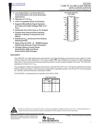
The CDC2351 is an integrated circuit that distributes one input clock signal to ten outputs with minimum skew. It features internal series damping resistors on each output to reduce transmission line effects and supports mixed-mode signal operation, allowing 5-V inputs/outputs while operating at a nominal 3.3-V supply voltage.
| Supply Voltage (VCC) | 3 V to 3.6 V |
|---|---|
| Operating Temperature Range | 0°C to 70°C |
| Input Clock Frequency (fCLK) | 100 MHz |
| High-Level Output Current (IOH) | -12 mA |
| Low-Level Output Current (IOL) | 12 mA |
Yes, it supports 5-V input and output voltages while operating at a nominal 3.3-V supply voltage.
The CDC2351 is a high-performance clock-driver circuit that distributes one input clock signal to ten outputs with minimum skew.
The CDC2351 operates with a supply voltage between 3 V and 3.6 V.
The CDC2351 is characterized for operation from 0°C to 70°C.