
The CDC2516 3.3-V Phase-Lock Loop Clock Driver is a high-performance, low-skew, low-jitter, phase-lock loop (PLL) clock driver. It uses a PLL to precisely align, in both frequency and phase, the feedback output (FBOUT) to the clock (CLK) input signal. It is specifically designed for use with synchronous DRAMs. The CDC2516 operates at 3.3-V VCC and provides integrated series-damping resistors that make it ideal for driving point-to-point loads. Four banks of four outputs provide 16 low-skew, low-jitter copies of the input clock. Output signal duty cycles are adjusted to 50 percent, independent of the duty cycle at the input clock. Each bank of outputs can be enabled or disabled separately via the 1G, 2G, 3G, and 4G control inputs. When the G inputs are high, the outputs switch in phase and frequency with CLK; when the G inputs are low, the outputs are disabled to the logic-low state. Unlike many products containing PLLs, the CDC2516 does not require external RC network.
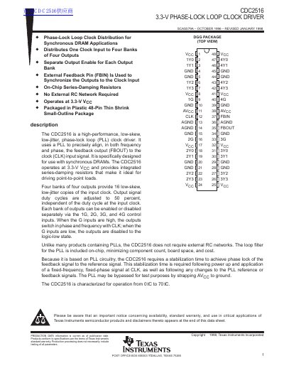
The CDC2516 is a high-performance, low-skew, low-jitter phase-locked loop (PLL) clock driver specifically designed for use with synchronous DRAMs. It distributes one clock input to four banks of four outputs, providing 16 low-skew copies of the input clock. Each output bank can be enabled or disabled separately via control inputs.
| Supply Voltage | 3.0 V to 3.6 V |
|---|---|
| Operating Temperature | 0°C to 70°C |
| Clock Frequency | 25 MHz to 125 MHz |
| Output Current (High) | 12 mA |
| Output Current (Low) | 12 mA |
| Package Type | 48-Pin Thin Shrink Small-Outline Package |
The stabilization time required for the integrated PLL circuit to obtain phase lock is 7 ms.
The device provides four banks of four outputs, totaling 16 low-skew copies of the input clock.
Yes, the PLL may be bypassed for test purposes by strapping AVcc to ground.