
The CDC2536 is a high-performance, low-skew, low-jitter clock driver. It uses a phase-lock loop (PLL) to precisely align, in both frequency and phase, the clock output signals to the clock input (CLKIN) signal. It is specifically designed for use with synchronous DRAMs and popular microprocessors operating at speeds from 50 MHz to 100 MHz or down to 25 MHz on outputs configured as half-frequency outputs. The CDC2536 operates at 3.3-V VCC and is designed to drive a 50-Ω transmission line. The CDC2536 also provides on-chip series-damping resistors, eliminating the need for external RC network.
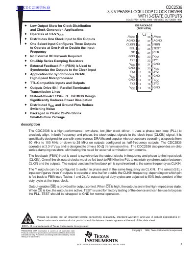
The CDC2536 is a high-performance, low-skew, low-jitter clock driver that uses a phase-lock loop (PLL) to align clock output signals in frequency and phase to the input clock signal. It operates at 3.3 V and is specifically designed for use with synchronous DRAMs and popular microprocessors operating at speeds from 50 MHz to 100 MHz. The device distributes one clock input to six outputs and includes on-chip series-damping resistors to eliminate the need for external termination components.
The CDC2536 features a voltage-controlled oscillator (VCO) with a frequency range of 100 MHz to 200 MHz. Outputs can be configured to operate at one-half, one-fourth, or double the input frequency depending on the SEL input and feedback configuration. The device is characterized for operation from 0°C to 70°C and is packaged in a 28-pin Shrink Small-Outline Package (SSOP).
| Operating Temperature | 0°C to 70°C |
|---|---|
| VCO Frequency Range | 100 MHz to 200 MHz |
| Output Current (High) | -12 mA |
| Package Type | 28-Pin Shrink Small-Outline Package |
No, the CDC2536 does not require external RC networks because the loop filter for the PLL is included on-chip.
The CDC2536 requires a stabilization time to achieve phase lock of the feedback signal to the reference signal following power up or signal changes.
One of the six output clocks must be fed back to the FBIN pin for the PLL to maintain synchronization between the input and outputs.