
CDC208 is a clock driver produced by TI company, it can distribute one input signal to four output terminals with minimum jitter and high reliability.
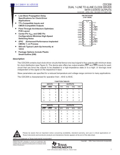
The CDC208 is a dual clock-driver circuit designed to fan out one input signal to four outputs with minimum skew for clock distribution. It features TTL-compatible inputs and CMOS-compatible outputs, utilizing a flow-through architecture to optimize PCB layout. The device includes two output-enable inputs for each circuit, allowing outputs to be disabled to a high-impedance state or forced to a high- or low-logic level independently of the input signal.
The CDC208 is characterized for operation from -40°C to 85°C and is available in a plastic small-outline (DW) package. It employs EPIC (Enhanced-Performance Implanted CMOS) 1.1µm process technology, offering 500-mA typical latch-up immunity. The datasheet provides detailed electrical characteristics, switching characteristics, function tables, and mechanical information for the 16-pin package.
| Operating temperature range | -40°C to 85°C |
|---|---|
| Supply voltage | 4.5 V to 5.5 V |
| High-level input voltage | 2 V |
| Low-level input voltage | 0.8 V |
| High-level output current | -24 mA |
| Low-level output current | 24 mA |
| Package type | Plastic Small-Outline (DW) |
The CDC208 contains dual clock-driver circuits that fan out one input signal to four outputs with minimum skew for clock distribution.
The device offers two output-enable inputs for each circuit that can force the outputs to be disabled to a high-impedance state or to a high- or low-logic level independent of the signal on the respective A input.
The recommended operating supply voltage is 5 V, with a range of 4.5 V to 5.5 V.