
The CDC2586 is a high-performance, low-skew, low-jitter clock driver. It uses a phase-lock loop (PLL) to precisely align, in both frequency and phase, the clock output signals to the clock input signals.
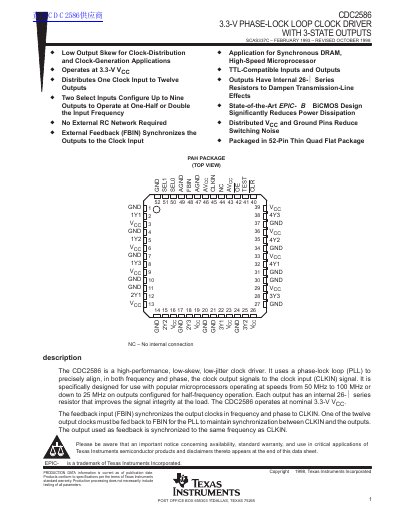
The CDC2586 is a high-performance, low-skew, low-jitter clock driver designed to distribute one clock input to twelve outputs. It utilizes an integrated phase-lock loop (PLL) to precisely align output signals in both frequency and phase with the CLKIN signal. The device operates at a nominal 3.3-V supply voltage and features TTL-compatible inputs and outputs.
| Supply Voltage | 3.3 V |
|---|---|
| Operating Temperature Range | 0°C to 70°C |
| Package Type | 52-Pin Thin Quad Flat Package |
No, unlike many products containing PLLs, the CDC2586 does not require external RC networks.
The CDC2586 is a high-performance clock driver that uses a phase-lock loop to align output signals with an input signal. It is specifically designed for use with microprocessors operating at speeds from 50 MHz to 100 MHz or down to 25 MHz on outputs configured for half-frequency operation.
A stabilization time is required following power up, application of a fixed-frequency signal at CLKIN, changes to reference or feedback signals, and enabling of outputs via OE.