
cdc203 is a 3.3v six-way switching circuit produced by texas instruments. It is suitable for applications requiring low skew between switching outputs. cdc203 adopts flow-through architecture, optimizes pcb layout, center-pin vcc and gnd pin configuration can minimize high-speed switching noise. The device is manufactured using 1-μm epic (enhanced performance implanted cmos) process, has a typical latch-up immunity of 500ma at 125℃, and is packaged in plastic small-outline package.
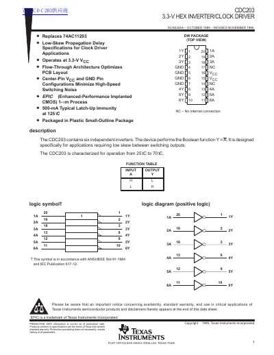
The CDC203 is a semiconductor device containing six independent inverters designed specifically for applications requiring low skew between switching outputs. It utilizes a flow-through architecture and EPIC CMOS 1-m process to optimize PCB layout and minimize high-speed switching noise. The device operates at a 3.3-V supply voltage and is characterized for operation from 25°C to 70°C.
| Supply Voltage | 3.3 V |
|---|---|
| Operating Temperature | 25°C to 70°C |
| Number of Inverters | Six |
It contains six independent inverters designed specifically for applications requiring low skew between switching outputs.
The recommended supply voltage is 3.3 V, with a range from 3.0 V to 3.6 V.