
This application note introduces the MicroFET 1.6x1.6 package technology, including MLP technology, package design, and assembly process
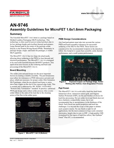
This application note provides assembly guidelines for the Fairchild MicroFET 1.6x1.6mm package, which is based on Molded Leadless Packaging (MLP) technology. The document focuses on soldering and back-end processing to ensure reliable performance in power-related applications.
Key topics include PWB design considerations such as pad dimensions and material selection (lead-free FR-4), stencil design for paste printing, and the use of specific lead-free solder pastes like SAC 305. The note also details reflow profiles, voiding criteria (suggesting a maximum of 25% macro voiding), and recommendations regarding component reuse after rework.
| Package Technology | Molded Leadless Packaging (MLP) |
|---|---|
| Peak Reflow Temperature | 260°C |
| Maximum Macro Voiding | 25% |
| Recommended Solder Alloy | SAC 305 (96.5Sn/3.0Au/0.5Cu) |
| Recommended PWB Material | Lead-free FR-4 |
Fairchild suggests a maximum of 25% voiding for MLP type packages based on reliability studies.
No, it is recommended that the component not be reused if rework becomes necessary due to high temperatures.
The industry standard SAC 305 (96.5Sn/3.0Au/0.5Cu) lead-free solder paste is the choice.