
This document introduces the features and characteristics of the QFET product, which can be used for digital control of circuits.
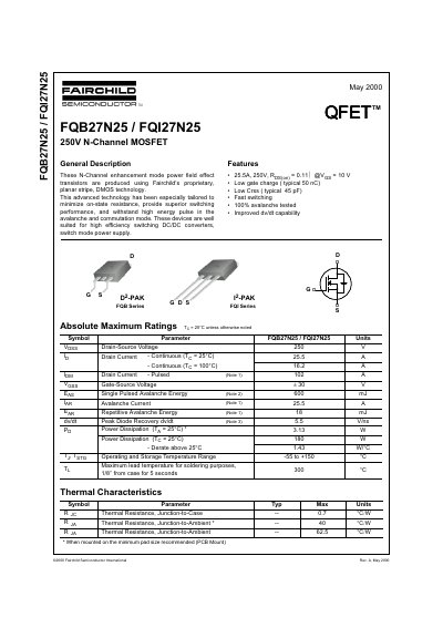
This document is a datasheet for the Fairchild FQB27N25 and FQI27N25 N-Channel enhancement mode power field effect transistors. These devices utilize Fairchild's proprietary planar stripe, DMOS technology to minimize on-state resistance and provide superior switching performance. They are well-suited for high efficiency switching DC/DC converters and switch mode power supply applications.
| Drain-Source Voltage | 250 V |
|---|---|
| Continuous Drain Current (Tj = 25°C) | 25.5 A |
| Continuous Drain Current (Tj = 100°C) | 16.2 A |
| Pulsed Drain Current | 102 A |
| Gate-Source Voltage | +30 V |
| Single Pulsed Avalanche Energy | 600 mJ |
| Power Dissipation (Ta = 25°C) | 3.13 W |
| Power Dissipation (Tc = 25°C) | 180 W |
| Operating and Storage Temperature Range | -55 to +150 °C |
| On-Resistance | 0.11 Ω |
| Input Capacitance | 2450 pF |
| Output Capacitance | 470 pF |
| Turn-On Delay Time | 75 ns |
| Turn-Off Delay Time | 170 ns |
| Total Gate Charge | 65 nC |
These devices are produced using Fairchild's proprietary, planar stripe, DMOS technology.
They are well suited for high efficiency switching DC/DC converters and switch mode power supply applications.
Yes, the devices are 100% avalanche tested.
The maximum lead temperature for soldering purposes is 300°C for 1/8" from case for 5 seconds.