
This document describes the features and characteristics of the FDS9958 Dual P-Channel PowerTrench® MOSFET, including maximum on-state resistance, low gate charge, and suitability for portable electronics applications.
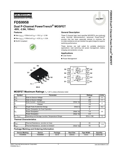
The FDS9958 is a dual P-channel logic level specified MOSFET produced using Fairchild Semiconductor's advanced PowerTrench process. It is designed to minimize on-state resistance while maintaining low gate charge for superior switching performance. These devices are well suited for portable electronics applications, specifically for load switching and power management, battery charging, and protection circuits.
| Drain to Source Voltage | -60 V |
|---|---|
| Gate to Source Voltage | ±20 V |
| Pulsed Drain Current | -12 A |
| Power Dissipation for Dual Operation | 2 W |
| Operating Junction Temperature Range | -55 to +150 °C |
| Thermal Resistance, Junction to Case | 40 °C/W |
| Package Type | SO-8 |
The device is well suited for portable electronics applications including load switching, power management, battery charging, and protection circuits.
The maximum on-state resistance is 105mΩ when VGS is -10V and ID is -2.9A.
Yes, the datasheet lists the device as RoHS Compliant.