
This document describes the features and characteristics of FDMB3900AN Dual N-Channel Power Trench® MOSFETTM, including maximum resistance, switching speed, etc.
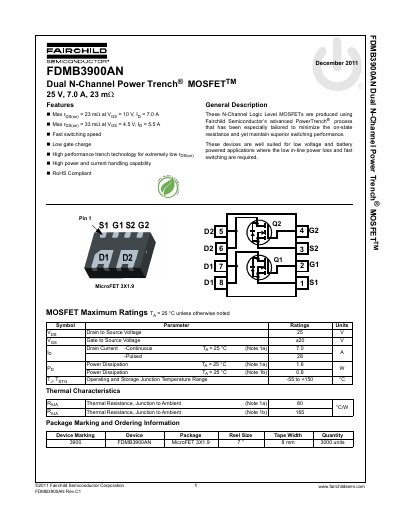
This document is a datasheet for the Fairchild Semiconductor FDMB3900AN, a Dual N-Channel Power Trench MOSFET. The device is produced using Fairchild Semiconductor's advanced PowerTrench process and is designed for low voltage and battery powered applications requiring low in-line power loss and fast switching.
The FDMB3900AN features a maximum drain to source voltage of 25V and a continuous drain current of 7.0A. Key electrical characteristics include a static drain to source on resistance of 23 mΩ at Vgs = 10V and 38 mΩ at Vgs = 4.5V. The device is RoHS Compliant and is available in the MicroFET 3X1.9 package.
| Package Type | MicroFET 3X1.9 |
|---|
Yes, the device is RoHS Compliant.
The device supports a continuous drain current of 7.0 A at 25 °C.
The maximum power dissipation is 1.6 W when mounted on a 1 in² pad of 2 oz copper.
The device operates within a junction temperature range from -55 to +150 °C.