
FDG6318P is a dual P-Channel logic level enhancement mode MOSFET produced by Fairchild Semiconductor using the PowerTrench process, with a small resistance, suitable for low voltage applications
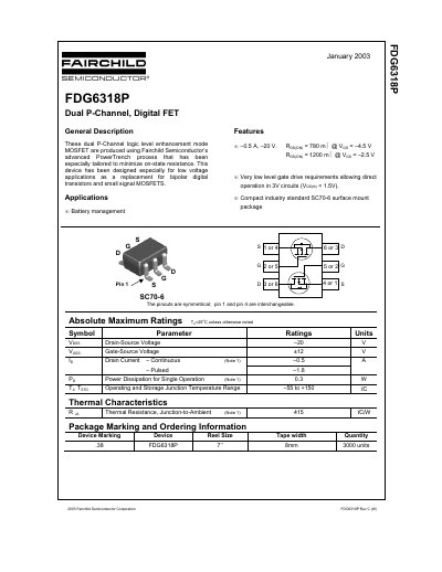
The Fairchild FDG6318P is a dual P-Channel logic level enhancement mode MOSFET produced using the PowerTrench process. It is specifically designed for low voltage applications as a replacement for bipolar digital transistors and small signal MOSFETs, featuring very low gate drive requirements allowing direct operation in 3V circuits.
The device is available in a compact industry standard SC70-6 surface mount package. Key electrical characteristics include a maximum continuous drain current of -0.5 A, a maximum drain-source voltage of -20 V, and a maximum power dissipation of 0.3 W for single operation. The pinouts are symmetrical, with pin 1 and pin 4 being interchangeable.
| Drain-Source Voltage | -20 V |
|---|---|
| Gate-Source Voltage | +12 V |
| Drain Current (Continuous) | -0.5 A |
| Power Dissipation (Single) | 0.3 W |
| Operating Temperature Range | -55 to +150 °C |
| Thermal Resistance (Junction-to-Ambient) | 415 °C/W |
| Package Type | SC70-6 |
The maximum continuous drain current is -0.5 A.
Yes, the pinouts are symmetrical; pin 1 and pin 4 are interchangeable.
The minimum gate threshold voltage is 0.65 V.