
This is a document about FDG6318PZ dual P-channel digital enhancement mode MOSFET. The product features low on-state resistance and low gate drive requirements, suitable for battery management and other applications.
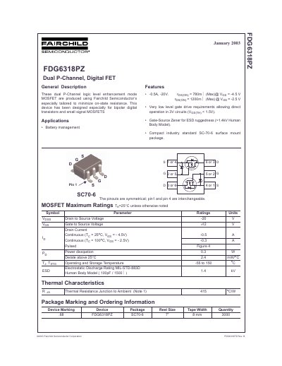
This document is a technical datasheet for the Fairchild Semiconductor FDG6318PZ, a dual P-Channel logic level enhancement mode MOSFET. The device features very low gate drive requirements allowing direct operation in 3V circuits and includes Gate-Source Zener protection for ESD ruggedness.
The datasheet provides comprehensive electrical characteristics including off-state breakdown voltage, on-resistance, capacitance, and switching times. It also details thermal ratings, safe operating areas, and typical characteristic curves such as normalized power dissipation versus temperature.
| Drain to Source Voltage (VDS) | -20 V |
|---|---|
| Gate to Source Voltage (VGS) | +/- 2 V |
| Continuous Drain Current (ID) at Tj=25°C | -0.5 A |
| Power Dissipation (PD) | 0.3 W |
| Operating and Storage Temperature Range | -55 to 150 °C |
| ESD Human Body Model Rating | >1.4 kV |
The maximum continuous drain current is -0.5 A when the junction temperature is 25°C and VGS is -4.5V.
The device has very low level gate drive requirements allowing direct operation in 3V circuits with VGG(TH) less than 1.5V.
Yes, the pinouts are symmetrical; pint and pin 4 are interchangeable.