
This document introduces the FDD3690 model N-channel power MOSFET, which is designed to improve the overall efficiency of DC/DC converters. It features faster switching and lower gate charge compared to other MOSFETs with similar RDS(ON) specifications. It is suitable for synchronous or conventional switching PWM controllers. The MOSFET is easy and safer to drive, even at very high frequencies, and enables DC/DC power supply designs with higher overall efficiency.
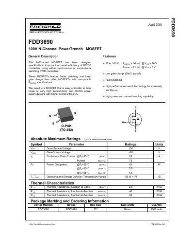
The FDD3690 is an N-Channel MOSFET designed to improve the efficiency of DC/DC converters using synchronous or conventional switching PWM controllers. It features faster switching, lower gate charge, and high performance trench technology for extremely low on-resistance. The device is available in a D-PAK (TO-252) package.
| Drain-Source Voltage | 100 V |
|---|---|
| Continuous Drain Current @Tc=25°C | 22 A |
| Power Dissipation @Tc=25°C | 60 W |
| Operating and Storage Junction Temperature Range | -55 to +175 °C |
| Thermal Resistance, Junction-to-Case | 2.5 °C/W |
| Thermal Resistance, Junction-to-Ambient (Note 1a) | 40 °C/W |
| Thermal Resistance, Junction-to-Ambient (Note 1b) | 96 °C/W |
| Package Type | D-PAK (TO-252) |
| Gate Charge (Typical) | 28 nC |
It is designed specifically to improve the overall efficiency of DC/DC converters using either synchronous or conventional switching PWM controllers.
Key features include fast switching, low gate charge (28nC typical), high performance trench technology for low on-resistance, and high power and current handling capability.
The operating and storage junction temperature range is from -55 to +175 °C.