
The IDT2309A is a 3.3V zero delay clock buffer designed for high-speed clock distribution applications. The device operates within the range of 10 to 133MHz and distributes one clock input to one bank of five and one bank of four outputs. Each output bank has a separate enable signal. The output skew is less than 250ps, and the jitter is less than 200 ps. The device is available in standard drive (IDT2309A-1) and high drive (IDT2309A-1H) versions. No external RC network is required, and the device operates at 3.3V VDD. The device is available in SOIC and TSSOP packages.
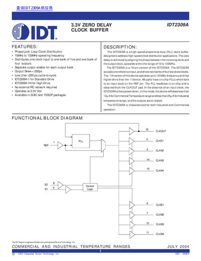
The IDT2309A is a high-speed phase-lock loop (PLL) clock buffer designed for high-speed clock distribution applications. It accepts one reference input and drives two banks of four low-skew clocks, achieving zero delay by aligning the phase between incoming and output clocks within the 10 to 133MHz range.
The device is available in -1 (Standard Drive) and -1H (High Drive) versions and operates at a 3.3V supply voltage. It features separate output enable for each bank, low jitter less than 200 ps cycle-to-cycle, and output skew less than 250ps. The IDT2309A is characterized for both Commercial (0°C to +70°C) and Industrial (-40°C to +85°C) temperature ranges.
| Operating Frequency Range | 10MHz to 133MHz |
|---|---|
| Supply Voltage | 3.3V VDD |
| Output Skew | < 250ps |
| Cycle-to-Cycle Jitter | < 200 ps |
| Package Types | SOIC and TSSOP |
| Industrial Temperature Range | -40°C to +85°C |
The device operates within a frequency range of 10 to 133MHz.
In power down mode, the device draws less than 12uA for the Commercial temperature range.
The maximum output-to-output skew is 250 ps when all outputs are equally loaded.